Key points of this research result
- World's first elucidation of band structure and spin state inside iron nitride "Fe₄N", which is attracting attention as a next-generation memory material
- A powerful guide to device development in the field of spintronics that exhibits higher performance and material exploration through theoretical calculations.
- Realized using Hiroshima University's Institute of Synchrotron Radiation Science (commonly known as HiSOR)
overview
Hiroshima University Graduate School of Advanced Science and Engineering, Chiral Knot Supermaterial Center Contributing to Sustainability (WPI-SKCM)2) Professor Akio Kimura's research group, in collaboration with Professor Taichi Okuda of Hiroshima University's Institute of Synchrotron Radiation Research (HiSOR), Principal Researcher Shinji Isogami, and Principal Researcher Keisuke Masuda of the National Institute for Materials Science, has revealed for the first time in the world iron nitride "Fe₄N" (*1), which is attracting attention as a material for next-generation energy-saving electronic devices. This result provides design guidelines for spintronic materials (*2), which are expected to be used as next-generation low-power devices.
The results of this research were published in Physical Review Research, a journal of the American Physical Society, on June 8, 2026.
Paper information
Paper title: Visualizing bulk band structure in Fe4N thin-films by spin- and angle-resolved photoelectron spectroscopy
Author name: Kaede Nakanishi1, Masaaki Kanokogi1, Kiyotaka Owada1,Kenta Kuroda1,2, Kazuki Tsunoda3, Hitoshi Sato3, Koji Miyamoto3, Taichi Okuda2,3, *Shinji Isogami4, *Keisuke Masuda4, Yuya Sakuraba4, *Akio Kimura1,2(*Corresponding author)
Affiliation:1Hiroshima University Graduate School of Advanced Science and Engineering,2Hiroshima University Super Materials Center Contributing to Sustainability (WPI-SKCM2),3Hiroshima University Institute of Synchrotron Radiation Science,4National Institute for Materials Science
DOI: 10.1103/mlcy-gszb
background
The electronic devices around us use "electronic charge." On the other hand, electrons also have a property called "spin" (*3), which acts like a small magnet. The technology that utilizes this spin isspintronicsis. For example, hard disk (HDD) read heads and magnetic memory (MRAM) use the phenomenon that electrical resistance changes depending on the spin direction (TMR).
Iron (Fe) is a typical ferromagnetic material that has been known for a long time. However, when nitrogen (N) enters the crystal and forms a special structure called an "inverted perovskite structure," the way electrons flow and the spin state change significantly. In particular, iron nitride Fe₄N has been theoretically predicted to have the possibility of exhibiting "100% negative spin polarization" (*4), and has attracted worldwide attention as a next-generation spintronics material. But actuallyUntil now, it has not been directly observed what kind of electronic states and spin states are formed.This research also clarifies how the structure of a material produces its properties and functions. In other words, Fe₄N is a good example of a material's structure changing the spin state of the electrons and creating new functions. This research aims to clarify this relationship through direct observation of electronic states and spin states.
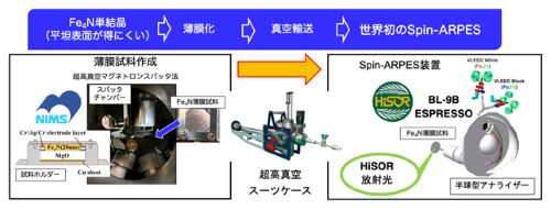
Figure 1: At the National Institute for Materials Science (NIMS), Fe4N thin films were prepared by ultra-high vacuum magnetron sputtering, transported from NIMS to HiSOR at the Institute for Synchrotron Radiation Science using a portable vacuum transport chamber without exposure to the atmosphere, and subjected to spin and angle-resolved photoelectron spectroscopy.
Contents of research results
This research team has investigated iron nitride Fe, which is expected to have a large negative spin polarization of conduction electrons.4Focusing on N, we performed a spin/angle-resolved photoelectron spectroscopy experiment (*6) using synchrotron radiation (*5) at Hiroshima University's Institute of Synchrotron Radiation Science (HiSOR) to clarify the band structure and its spin state. Generally, angle-resolved photoelectron spectroscopy experiments require a sample with a flat and clean surface in ultra-high vacuum. However, Fe4Due to the three-dimensional crystal structure of bulk single crystals of N, it is difficult to obtain a flat surface in vacuum, and angle-resolved photoelectron spectroscopy experiments have rarely been performed to date. Therefore, in this research, we collaborated with Principal Researcher Shinji Isogami of the National Institute for Materials Science (NIMS) to investigate Fe, which has an atomically flat surface and large residual magnetization.4The N thin film was created using ultra-high vacuum magnetron sputtering. To prevent surface contamination of the thin film sample, the sample was transported from NIMS to HiSOR at the Institute for Synchrotron Radiation Science using a portable vacuum transport chamber without being exposed to the atmosphere, and spin-angle-resolved photoelectron spectroscopy was performed (Figure 1). This allows Fe to have a flat and clean surface.4For the first time, experiments using N single crystal samples are now possible.
As a result, Fe4N'sFirst successful observation of bulk-derived band structure(Figure 2). Specifically, at around -0.2 eV near the Fermi level (*7), we observed an electron pocket A that crosses the Fermi level and a parabolic band B that is in contact with it (upper left of Figure 2). Spin-resolved measurements show that both electron pocket A and the adjacent parabolic band B have negative spin polarization, which leads us to conclude that they originate from minority spins (Figure 2, right). Furthermore, as a result of spin decomposition across all wavenumbers, it was revealed that all other band structures observed were derived from minority spins (Figure 2, lower left).
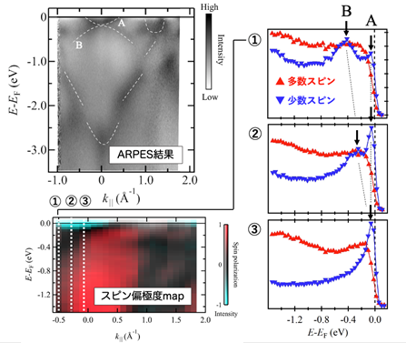
Figure 2:Fe4Experimental results of spin and angle-resolved photoelectron spectroscopy of N thin films. An electron pocket A crossing the Fermi level (*5) and a parabolic band B in contact with it were observed at around -0.2 eV near the Fermi level. Spin-resolved measurements show that both electron pocket A and the parabolic band B in contact with it have negative spin polarization, so they can be attributed to minority spins. Furthermore, as a result of spin decomposition across all wavenumbers, it was revealed that all other observed band structures were derived from minority spins.
Future developments
Fe₄N is theoretically predicted to exhibit an extremely large TMR effect, and is expected to be applied to next-generation MRAM and ultra-low power spintronic devices. This research revealed that conduction is dominated by "minority spin" electrons, which have spin angular momentum in the opposite direction to the spin that determines the magnet's north-south pole direction (magnetization direction). In such electronic states, it is possible to efficiently utilize the "spin transfer torque (*8)" effect, which uses the spin angular momentum of conduction electrons to control the magnetization direction. Therefore, it is expected to be applied to new MRAM writing technology and microwave oscillation elements for next-generation HDDs.
Terminology explanation
*1. Iron nitride (Fe₄N)
A material made from iron (Fe) and nitrogen (N). It has the potential to efficiently utilize the "magnetic properties (spin)" of electrons, and is expected to be applied to next-generation energy-saving memories and electronic devices.
*2. spintronics
A next-generation electronic technology that utilizes the spin (orientation of a magnet) of electrons. It is expected to achieve faster speeds and lower power consumption.
*3. electron spin
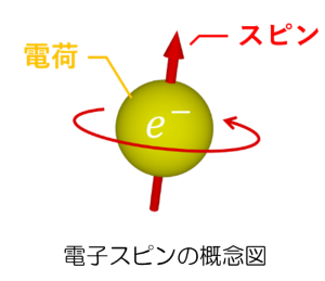
In addition to its properties as an electric charge, electrons also have properties as magnets due to their rotation. This is called electron spin, and the direction of rotation is expressed by direction, and it can be divided into upward spin and downward spin. In the case of ferromagnetic materials (magnets), a magnetic force is generated because there is a difference in the number of upward spins for electrons rotating clockwise around the direction from the north pole to the south pole, and downward spins for electrons rotating in the opposite direction.
*4. Negative spin polarization, minority spin
When the number of electrons with upward (downward) spin is written as N↑(N↓), the spin polarization is defined as P=(N↑-N↓)/(N↑+N↓).
In magnetic materials, the number of electrons may vary depending on the direction of the electron spin. Spins in the direction of more electrons are called "majority spins" and spins in the direction of fewer electrons are called "minority spins." Now, take the opposite direction of magnetization as "positive". In ordinary iron, majority-spin electrons are responsible for conduction and ``conduction electrons are positively spin-polarized.'' However, in Fe₄N, minority-spin electrons are mainly involved in conduction and are thought to be negatively spin-polarized, which is the origin of the unique spintronic properties. Normally, N↑(N↓) is the number of majority spins (minority spins), so if only minority spin electrons are responsible for electrical conduction, P=-1 (-100%), which is said to be ``100% negatively spin-polarized conduction electrons.''
*5. synchrotron radiation
When electrons that have been accelerated to the speed of light are bent by a magnetic field, intense light called synchrotron radiation is generated. In space, synchrotron radiation can be found in nebulae, but on Earth it requires a dedicated accelerator. Synchrotron synchrotron radiation is the most powerful light available to humans and is also called "dream light." There are many synchrotron synchrotron radiation facilities in Japan, such as SPring-8, a large synchrotron radiation facility, and HiSOR, the only national university corporation's Hiroshima University Synchrotron Radiation Science Research Center, where cutting-edge research is being conducted.
*6. Spin-angle resolved photoelectron spectroscopy (Spin-ARPES)
When light shines on a material, electrons inside the material are emitted due to the photoelectric effect. At this time, the electrons that have not been scattered are emitted while retaining information about the electronic state inside the material according to the law of conservation of energy. Angle-resolved photoelectron spectroscopy is a method that directly observes the relationship between the binding energy and momentum of electrons inside a solid, that is, band dispersion, by analyzing the kinetic energy and emission angle of emitted electrons. Furthermore, by adding a spin detector, it is possible to separate and observe not only the kinetic energy and momentum of electrons, but also the electron spin (*3), making it possible to investigate the detailed electronic structure of magnetic materials. In this research, measurements are performed using a low-energy electron diffraction (VLEED) spin detector independently developed by the Institute of Synchrotron Radiation Science, Hiroshima University.
*7. Fermi level
Among the energy states occupied by electrons in a material, the highest energy state in which electrons can exist at absolute zero is called the Fermi level. In metals, electrons near the Fermi level are primarily responsible for electrical conduction, so this is a very important quantity in understanding the properties of electronic materials.
*8. spin transfer torque
When electrons with spin flow through a magnetic material, their spin angular momentum acts as a force (torque) in the direction of magnetization of the magnet, which can change the direction of magnetization. This phenomenon is called spin transfer torque. Since magnetization can be controlled only by current without using a magnetic field, it is expected to be applied to low power consumption magnetic devices such as MRAM.
Acknowledgment
This research was supported by the Japan Society for the Promotion of Science (JSPS) Grant-in-Aid for Scientific Research A, "Interfacial band observation by soft X-ray spin-resolved ARPES aimed at realizing high-performance multilayer magnetoresistive devices (Project number: 25H00743, Research representative: Akio Kimura), Academic Transformation Area Research (A)" This project was supported by Visualization, Design, and Creation of Quantum Materials Colored by Asymmetry (Project Number: 24H01670, 26H00671 Research Director: Akio Kimura).
- Press release materials (890.77 KB)
- Article publication journal (Physical Review Research)
- Hiroshima University Researcher Guidebook (Professor Akio Kimura)
[Regarding research]
Akio Kimura, Professor, Physics Program, Graduate School of Advanced Science and Engineering, Hiroshima University
Tel: 090-6346-5384
E-mail: akiok*hiroshima-u.ac.jp
[Regarding reporting]
Hiroshima University Finance and General Affairs Office, General Affairs and Public Relations Department, Public Relations Group
TEL: 082-424-4518 FAX: 082-424-6040
E-mail: koho*office.hiroshima-u.ac.jp
(Please replace * with half-width @)