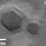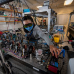
Researchers at Berkeley Lab recently unveiled a new, fast, and readily reproducible way to map and identify defects in two-dimensional materials. The method could dramatically reduce the time required to characterize two-dimensional materials and use them in next-generation quantum and electronic devices.